

All Products
-
Integrated Circuits (ICs)
- Integrated Circuits (ICs)
- AC to DC Converter ICs
- Active Filters
- ADC
- AFE
- Analog Multipliers & Dividers
- Analog Switches & Multiplexers ICs
- Application Specific Microcontrollers
- Application Specific Timer
- Audio Amplifiers
- Audio Special Purpose
- Battery Chargers ICs
- Battery Management ICs
- Buffers & Transceivers
- Capacitive Sensors
- Clock Buffers & Drivers
- Clock Generators
- CODECs Interface ICs
- Comparators
- Configuration Proms for FPGAs
- Controllers Interface ICs
- Converting Interface ICs
- Counters & Dividers
- CPLDs
- Current Regulator IC
- DAC
- DC DC Voltage Regulators
- DC to DC converter
- DDS
- Delay Lines Timing ICs
- Digital Potentiometers
- Display Drivers ICs
- Drivers Interface ICs
- DSP
- Embedded ICs Modules
- Energy Metering ICs
- FIFOs Memory
- Flip Flops
- FPGAs
- FPGAs with Microcontrollers
- Full & Half-Bridge Drivers ICs
- Gate Drivers ICs
- Gates & Inverters
- Hot Swap Controllers
- I/O Expanders
- IC Batteries
- Ideal Diode controller
- Instrumentational OP Amps
- Interface ICs Modules
- Laser Driver ICs
- Latches
- LED Driver ICs
- Lighting Controllers
- Linear Comparators
- Linear Regulator Controllers
- Linear Voltage Regulators
- Memory
- Memory Batteries
- Memory Controllers
- Microcontrollers
- Microprocessors
- Modems ICs & Modules
- Motor Drivers
- Multi-Functional Gates & Inverters
- Multivibrators
- Multivibrators
- PFC PMICs
- PLDs
- PoE Controllers
- Power Supply Control ICs
- Power Switches ICs
- Programmable Timers & Oscillators
- RMS to DC Converters
- RTCs
- Sensor & Detector Interface ICs
- Serializers & Deserializers
- Shift Registers
- Signal Buffers
- Signal Switches & Multiplexers
- Signal Terminators
- SoC
- Special Purpose ADCs/DACs
- Special Purpose Amplifiers
- Special Purpose Analog Switches
- Specialized ICs
- Specialized Interface ICs
- Specialized Power Management ICs
- Specialized Voltage Regulators
- Specialty Logic ICs
- Switching Voltage Regulators
- Telecom Interface ICs
- Thermal Management
- Touch Screen Controllers
- UARTs
- Universal Bus Functions
- V/F & F/V Converters
- Video Amps & Modules
- Video Processing Linear ICs
- Voice Record and Playback
- Voltage Reference
- Voltage Supervisors
- Voltage Translators & Level Shifters
-
Connectors
- Connectors
- ARINC Connectors
- Backplane Connector Contacts
- Backplane Connectors Accessories
- Backplane Connectors Housings
- Backshells and Cable Clamps
- Banana Tip Adapters
- Banana Tip Binding Posts
- Banana Tip Connectors Accessories
- Banana Tip Jacks
- Barrel Accessories
- Barrel Adapters
- Barrel Audio Connectors
- Barrel Connectors
- Barrel Power Connectors
- Barrier Terminal Blocks
- Between Series Adapters
- Blade Type Power Connectors
- Blade Type Power Connectors
- Blade Type Power Connectors Accessories
- Blade Type Power Connectors Housings
- Board In Connectors
- Board to Board Connectors
- Card Edge Adapters
- Card Edge Connectors Accessories
- Card Edge Connectors Housings
- Card Edge Contacts
- Centronics Connectors
- Circular Adapters
- Circular Connectors
- Circular Connectors Accessories
- Circular Connectors Housings
- Circular Contacts
- Coaxial Connectors
- Coaxial Connectors Accessories
- D-Sub Adapters
- D-Sub Connector Housings
- D-Sub Connector Terminators
- D-Sub Connectors
- D-Sub Connectors Accessories
- D-Sub Contacts
- D-Sub Hoods
- D-Sub Jackscrews
- DIN 41612 Connectors
- Din Rail Terminal Blocks
- Edgeboard Connectors
- Faceplates & Frames
- Fiber Optic Adapters
- Fiber Optic Connectors
- Fiber Optic Connectors Accessories
- Fiber Optic Connectors Housings
- Flat Flexible Connector Housings
- Flat Flexible Connectors
- Flat Flexible Connectors Accessories
- Flat Flexible Contacts
- Foil Connectors
- Hard Metric Connector
- Headers & Male Pins
- Heavy Duty Connectors Accessories
- Heavy Duty Connectors Assemblies
- Heavy Duty Connectors Frames
- Heavy Duty Connectors Housings
- Heavy Duty Connectors Modules
- Heavy Duty Contacts
- IC Adapters
- IC and Component Sockets
- IC Sockets Accessories
- Inline Memory Module Sockets
- Interface Modules Terminal Blocks
- Keystone Accessories
- Keystone Inserts
- Knife Connectors
- Leadframe Contacts
- LGH Connectors
- Magnetic Wire Terminals
- Magnetics Modular Jacks
- Memory Card Adapters
- Memory Card Sockets
- Memory Connectors Accessories
- Modular Adapters
- Modular Connectors Accessories
- Modular Jacks
- Modular Plug Housings
- Modular Plugs
- Multi Purpose Contacts
- Panel Mount Connectors
- Panel Mount Terminal Blocks
- PC Pin Terminals
- Photovoltaic Connectors
- Photovoltaic Connectors Accessories
- Photovoltaic Contacts
- Pluggable Connectors
- Pluggable Connectors Accessories
- Pluggable Terminal Blocks
- Power Distribution Terminal Blocks
- Power Entry Connectors Accessories
- Power Entry Connectors Modules
- Quick-Connect & Quick-Disconnect Connectors
- Rectangular Connectors
- Rectangular Connectors Accessories
- Rectangular Connectors Adapters
- Rectangular Connectors Arrays
- Rectangular Connectors Headers
- Rectangular Connectors Housings
- Rectangular Contact Inserts
- Rectangular Terminals
- RF Adapters
- RF Contacts
- RF Terminators
- Ring Terminals
- Screw Connectors
- Shunts & Jumpers
- Socket Terminals
- Solder Lug Connectors
- Spade Connectors
- Specialized Backplane Connectors
- Specialized Connectors
- Specialized Terminal Blocks
- Spring Loaded Contacts
- Spring Loaded Rectangular Connectors
- SSL Connectors
- SSL Connectors Accessories
- SSL Contacts
- Terminal Block Adapters
- Terminal Blocks - Contacts
- Terminal Blocks Accessories
- Terminal Jumpers
- Terminal Junction Systems
- Terminal Marker Strips
- Terminal Strips and Turret Boards
- Terminal Wire Ferrules
- Terminals Accessories
- Terminals Adapters
- Terminals Housings
- Transistor Sockets
- Turret Connectors
- Video Adapters
- Video Connector Accessories
- Video Connectors
- Wire Pin Connectors
- Wire Splice Connectors
- Wire-to-Board Connectors
- Wire-to-Board Terminal Blocks
- Wiring Blocks Accessories
- Wiring Modular Connectors
-
Discrete Semiconductors
- Discrete Semiconductors
- Arrays BJT Transistors
- BJT Transistors Arrays
- Bridge Rectifiers
- DIACs and SIDACs
- IGBTs Modules
- IGBTs Transistors Arrays
- JFETs Transistors
- MOSFETs Transistors Arrays
- Power Driver Modules
- Pre-Biased BJT Transistors
- Programmable Unijunction Transistors
- Rectifier Diode Array
- RF BJT Transistors
- RF Diodes
- RF MOSFETs Transistors
- SCRs Thyristors
- Single BJT Transistors
- Single IGBTs
- Single IGBTs
- Single MOSFETs Transistors
- Single-Phase Diode Rectifier
- Specialized Transistors
- Thyristors Modules
- TRIACs Thyristors
- Varactors
- Zener Diode Arrays
- Zener Single Diodes
-
Capacitors
- Capacitors
- Aluminum Electrolytic Capacitors
- Aluminum Polymer Capacitors
- Capacitor Accessories
- Capacitor Networks
- Ceramic Capacitors
- Ceramic Capacitors
- Film Capacitors
- Mica & PTFE Capacitors
- Niobium Oxide Capacitors
- Silicon Capacitors
- Supercapacitors & EDLC
- Tantalum Capacitors
- Tantalum Polymer Capacitors
- Thin Film Capacitors
- Trimmers Variable
-
Sensors
- Sensors
- CdS Cells
- Accelerometers
- Accessories
- Amplifiers
- Analog & Digital Sensor
- Analog & Digital Sensors
- Analog Optical Sensors
- Angle & Linear Position Measuring Sensors
- Camera Modules
- Color Sensors
- Current Sensors
- Distance Measuring Sensors
- Dust Sensors
- Encoders
- Float & Level Sensors
- Flow Sensors
- Force Sensors
- Gas Sensors
- Gyroscopes
- Humidity Sensors
- Image Sensors
- IMUs
- Inclinometers
- IrDA Transceiver Modules
- Junction Blocks
- Logic Optical Sensors
- Logic Photo Detectors
- Logic Photointerrupters
- LVDT Transducers
- Magnetic Compass Sensors Modules
- Magnetic Linear Sensors ICs
- Magnetic Position Sensors Modules
- Magnetic Switches
- Mechanical Temperature Sensors
- Multi Purpose Magnets
- Multifunction
- NTC Thermistors
- Occupancy Sensors
- Optical Motion Sensors
- Optical Sensors Remote Receiver
- Photodiodes
- Photoelectric Sensors
- Phototransistors
- Proximity Sensors
- PTC Thermistors
- RTD
- Sensor Cable Accessories
- Sensor Cable Assemblies
- Sensor Matched Magnets
- Shock Sensors
- Solar Cells
- Solid State Thermostats
- Specialized Sensors
- Strain Gauges
- Thermocouple Temperature Sensors
- Tilt Switch Sensors
- Touch Sensors
- Transducers
- Transistor Optical Sensors
- Ultrasonic Receivers
- UV Sensors
- Vibration Sensors
- Resistors
- Isolators
- Board Mount Poser Supplies
-
RF/IF & RFID
- RF/IF & RFID
- Attenuators
- Balun
- RF Accessories
- RF Amplifiers
- RF Antennas
- RF Boards
- RF Demodulators
- RF Detectors
- RF Directional Coupler
- RF Front End
- RF Misc ICs and Modules
- RF Mixers
- RF Modulators
- RF Multiplexers
- RF Power Controller ICs
- RF Power Dividers
- RF Receivers
- RF Shields
- RF Switches
- RF Transceiver ICs
- RF Transceiver Modules
- RF Transmitter
- RF Transmitters
- RFI & EMI Contacts
- RFI & EMI Materials
- RFID Accessories
- RFID Antennas
- RFID Boards
- RFID ICs
- RFID Reader Modules
- RFID Tags
- Circuit Protection
- Crystals
- Inductors
- Filters

CD4014BPWE4
You may place an order without registering to Utmel.
We strongly suggest you sign in before purchasing as you
can track your order in real time.
For your convenience, we accept multiple payment methods in USD, including PayPal, Credit Card, and wire transfer.
RFQ (Request for Quotations)It is recommended to request for quotations to get the latest
prices and inventories about the part.
Our sales will reply to
your request by email within 24 hours.
1. You'll receive an order information email in your inbox.
(Please remember to check the spam folder if you didn't hear from us).
2. Since inventories and prices may fluctuate to some
extent, the sales manager is going to reconfirm the order and let you know if there
are any updates.
Shipping starts at $40, but some countries will exceed $40. For
example (South Africa, Brazil, India, Pakistan, Israel, etc.)
The
basic freight (for package ≤0.5kg or corresponding volume) depends on the time zone and
country.
Currently, our products are shipped through DHL, FedEx, SF, and UPS.
Delivery TimeOnce the goods are shipped, estimated delivery time depends on the shipping methods you chose:
FedEx International, 5-7 business days.
The following are some common countries' logistic time.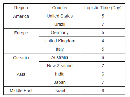
| Parameters | |
|---|---|
| Mount | Surface Mount |
| Package / Case | TSSOP |
| Number of Pins | 16 |
| Weight | 61.887009mg |
| Packaging | Rail/Tube |
| JESD-609 Code | e4 |
| Pbfree Code | yes |
| Moisture Sensitivity Level (MSL) | 1 |
| Number of Terminations | 16 |
| Terminal Finish | Nickel/Palladium/Gold (Ni/Pd/Au) |
| Max Operating Temperature | 125°C |
| Min Operating Temperature | -55°C |
| Additional Feature | OUTPUTS ALSO AVAILABLE AT 6TH AND 7TH STAGE OF THE SHIFT REGISTER; ALSO OPERATES AS SISO |
| Subcategory | Shift Registers |
| Technology | CMOS |
| Terminal Position | DUAL |
| Terminal Form | GULL WING |
| Peak Reflow Temperature (Cel) | 260 |
| Number of Functions | 1 |
| Supply Voltage | 5V |
| Terminal Pitch | 0.65mm |
| Pin Count | 16 |
| Operating Supply Voltage | 15V |
| Temperature Grade | MILITARY |
| Number of Circuits | 1 |
| Max Supply Voltage | 18V |
| Min Supply Voltage | 3V |
| Number of Bits | 8 |
| Propagation Delay | 120 ns |
| Turn On Delay Time | 320 ns |
| Logic Function | OR, Shift Register |
| Direction | Unidirectional |
| Output Polarity | TRUE |
| Logic IC Type | PARALLEL IN SERIAL OUT |
| Trigger Type | POSITIVE EDGE |
| Number of Input Lines | 9 |
| Number of Output Lines | 3 |
| Length | 5mm |
| Width | 4.4mm |
| Radiation Hardening | No |
| RoHS Status | RoHS Compliant |
| Lead Free | Contains Lead |
CD4014BPWE4 Overview
There is an embedded device in the package TSSOP. 16 is the total number of terminations on the chip. This item is packed in case Rail/Tube. The part operates at 5V voltage. The device is equipped with 16 pins. Mounting by Surface Mount is recommended. It's noted that the chip's operating supply voltage is in the range 15V. The following additional aspects of this section are worth noting: OUTPUTS ALSO AVAILABLE AT 6TH AND 7TH STAGE OF THE SHIFT REGISTER; ALSO OPERATES AS SISO. This device has 9 input lines available. IC chip bits total 8. This board has 16 pins in total. The product should be used at temperatures below 125°C. In order for this device to function, the value should not be less than -55°C. 18V is the supply voltage used. This supply voltage is employed higher than 3V. A total of 3 output lines are available for operation. The subcategory in which it falls belongs to is Shift Registers. There are 1 circuits in this device.
CD4014BPWE4 Features
With 16 pins
Operate supply voltage at 15V
With 3 output lines
CD4014BPWE4 Applications
There are a lot of Texas Instruments CD4014BPWE4 Shift Registers applications.
- Parallel to serial converter
- LED matrix control
- Generate time delay toward digital circuits
- Delay Line
- data transfer
- 7-segment display control
- Pattern Recognizers
- Flash Memory
- ROM Chips
- temporary data storage